On April 12th, Associate Professor Lu Fang from Department of Electronic Engineering and Professor Qionghai Dai from Department of Automation, reported an innovation of photonic AI chiplet “Taichi”, empowering 160 TOPS/W artificial general intelligence. The research has been published on Science.
The rapid development in the field of artificial general intelligence (AGI) imposes stringent energy efficiency and area efficiency requirements on next-generation computing. As a brand-new technology to break the plateauing of Moore’s Law, integrated photonic neural networks have shown great potential in achieving superior processing speed and high energy efficiency. However, it suffers severely limited computing capability and scalability that only simple tasks and shallow models (e.g., 4-class vowels classification, 10-category digits classification, etc., with up to thousand-parameter-level networks) were experimentally realized in photonic integrated circuits, hardly supporting modern AGIs.

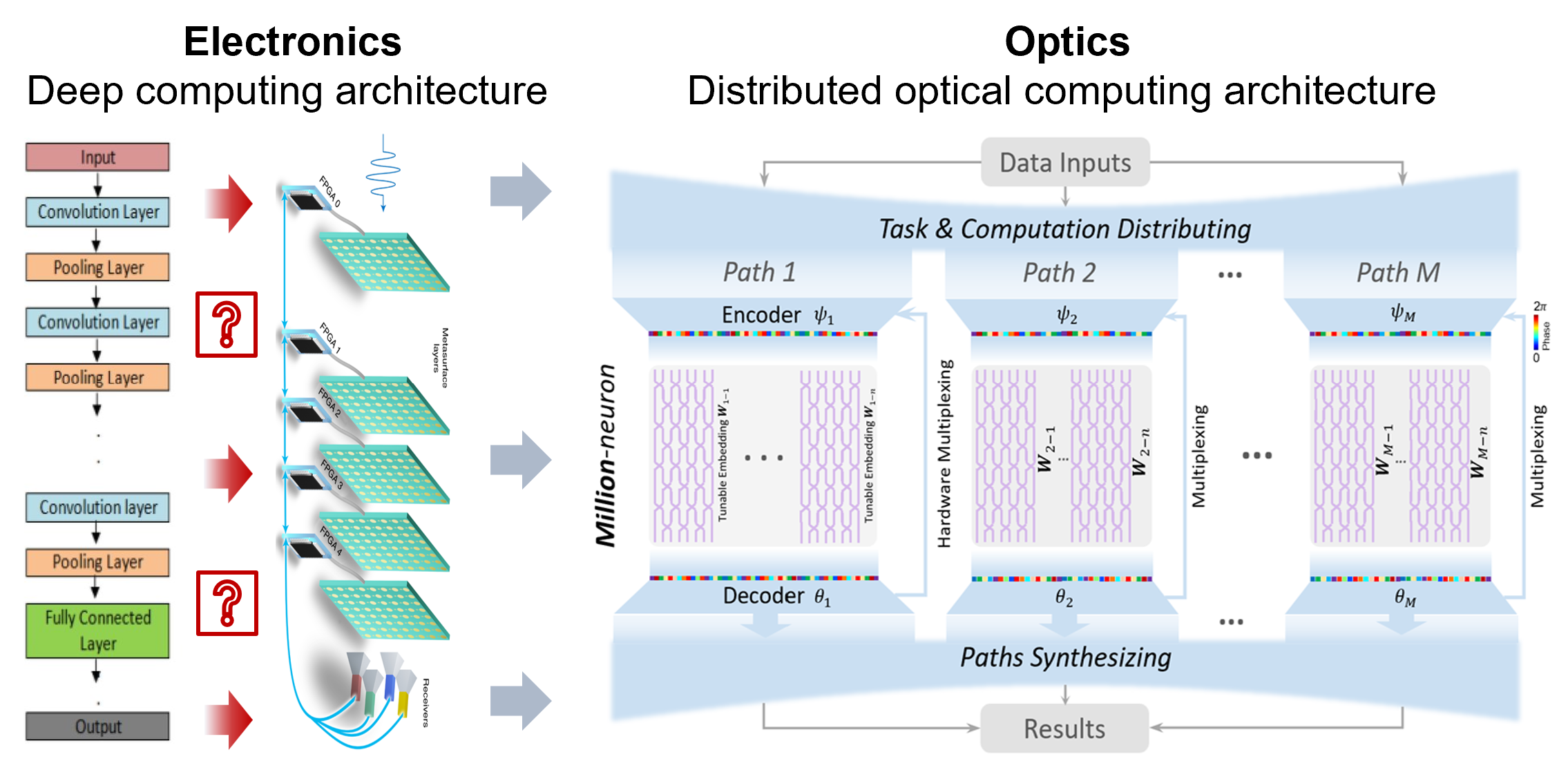
Distributed optical computing architecture - Taichi.
The research team innovated Taichi, a large-scale photonic AI chip along with a distributed optical computing architecture, owning billions-of-neuron on-chip computing capability with 160-TOPS/W energy efficiency. Taichi not only exploits the high parallelism and high connectivity of wave optics to implement computing with very high computing density, but also explores a general and iterative encoding-embedding-decoding photonic computing to effectively increase the scale of the optical neural network to billion neuron level. For the first time, Taichi experimentally realizes on-chip large optical neural networks for thousand-category-level classification and artificial intelligence-generated content (AIGC) tasks, with up to 2-3 orders of magnitude improvement in area efficiency and energy efficiency compared to current AI chips.

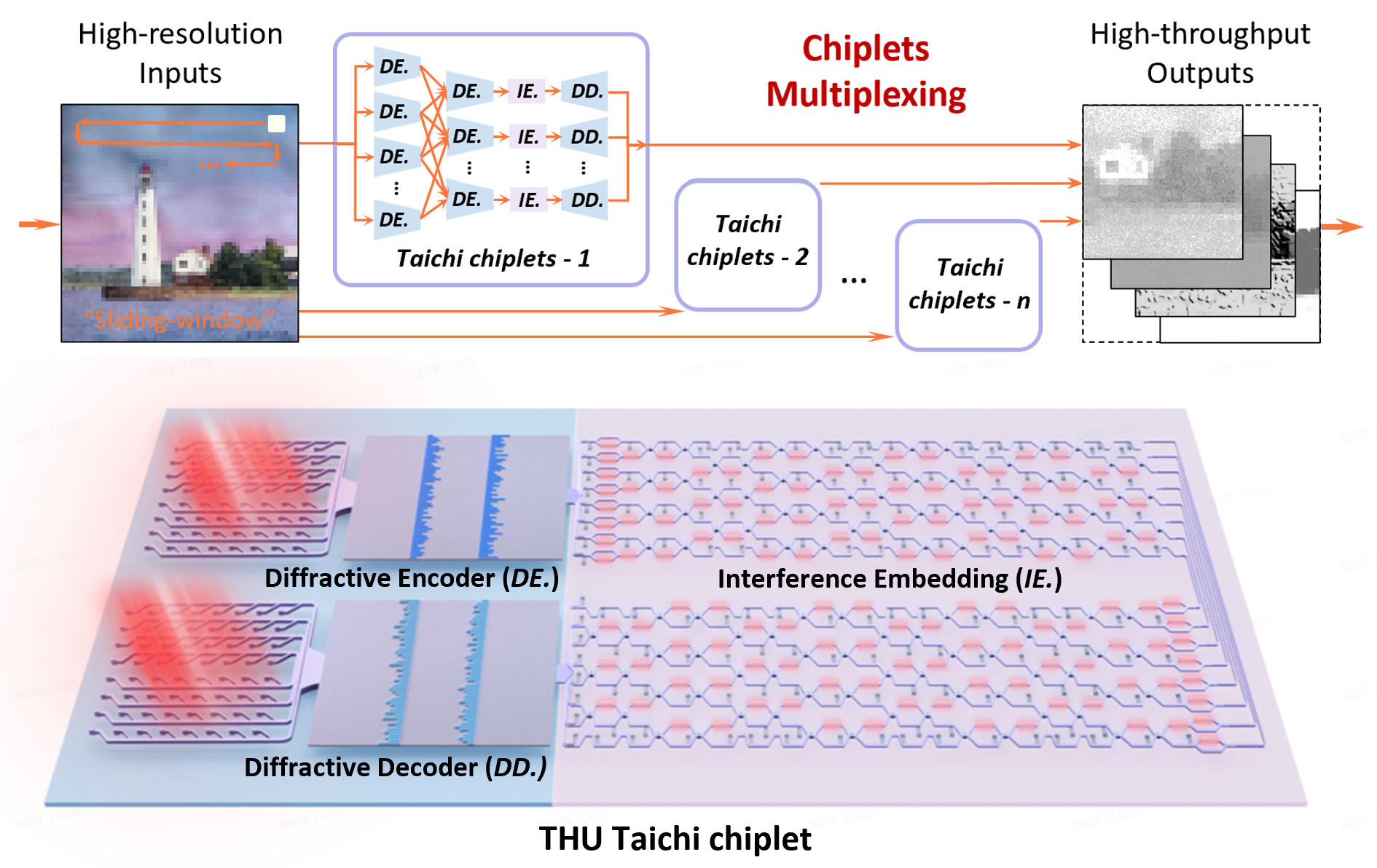
The integrated large-scale interference-diffraction-hybrid photonic chiplet
The innovations of Taichi are as follows. 1. We proposed a universal and robust distributed computing protocol for complex AGI tasks. Instead of going deeper as electronic computing, Taichi architecture goes broad for throughput and scale expansion. A binary encoding protocol is proposed to divide challenging computing tasks and large network models into sub-problems and sub-models that can be distributed and deployed on photonic chiplet. This atomic divide-and-concur operation enables large-scale tasks to be adaptively solved with flexible scales, achieving on-chip networks with up to 10 billion of optical neurons. 2. We developed the largest-scale photonic chiplets to support input and output dimensions as large as 64 × 64. By integrating scalable wavefield diffraction and reconfigurable interference, the entire inputs are encoded passively and modulated in a highly-parallel way, achieving 160 TOPS/W on-chip energy efficiency and 879 T MACS/mm² area efficiency (up to 2 orders of magnitude improvement in both energy and area efficiency than existing AI chips). 3. We demonstrated the versatility and flexibility of Taichi via on-chip experiments with state-of-the-art performances: 1) an accuracy of 91.89% in 1623-category Omniglot characters classification and 87.74% in 100-category mini-ImageNet classification, 2) the on-chip high-fidelity AIGC models are demonstrated such as music composing and high-resolution styled paintings generation.
Taichi not only breaks the scale limitation towards beyond-billion-neurons foundation model with large-scale high-throughput photonic chiplets, but also achieves error-prone robustness through information scattering and synthesizing. As the largest-scale photonic AI chip, Taichi experimentally solved the complex on-chip AGI tasks (thousand-category-level classifications and various-modality AIGC), leading to a giant leap in scalability, accuracy and efficiency. The breakthrough of Taichi paves a viable route to real-world photonic computing and represents an important step for next-generation high-efficiency AI chips, supporting applications in large machine learning models, AIGC, robotics, etc.
Source: Department of Electronic Engineering
Editor: Guo Lili